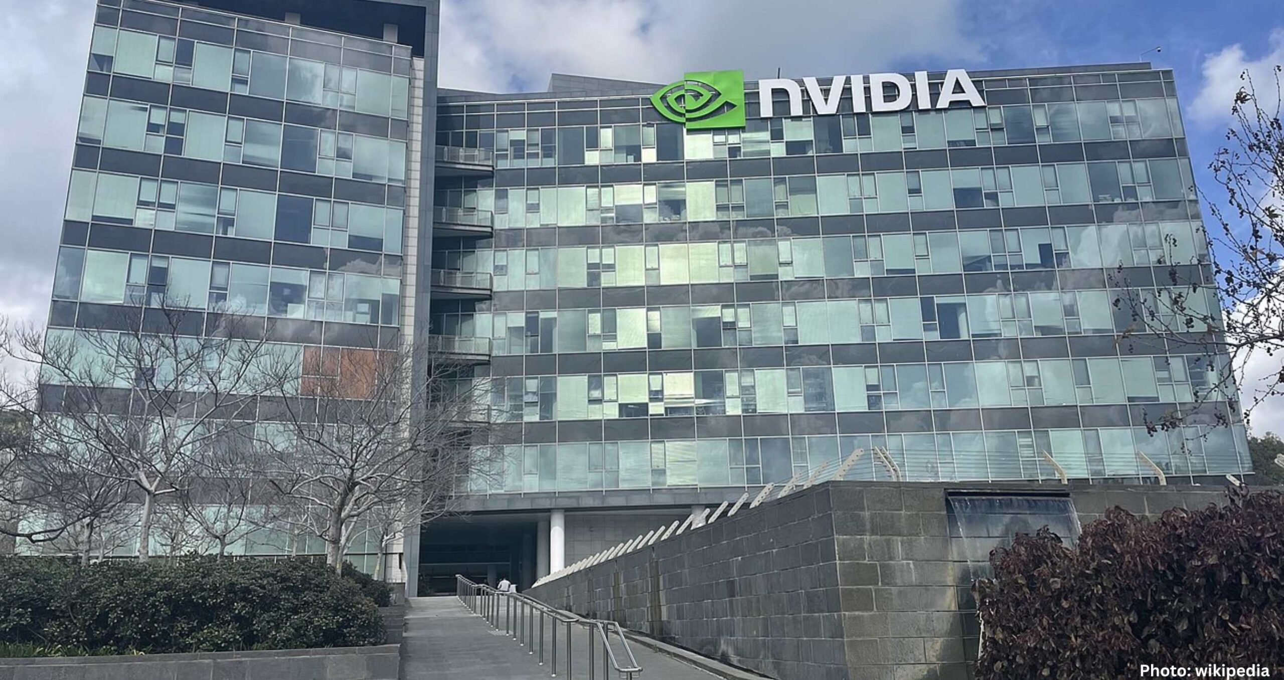
Nvidia has unveiled its first Blackwell chip wafer produced in the U.S. at TSMC’s Phoenix facility, marking a significant advancement in American semiconductor manufacturing and AI technology.
Nvidia has announced the production of its first Blackwell chip made in the United States at TSMC’s semiconductor manufacturing facility in Phoenix, Arizona. This event signifies a pivotal moment in the evolution of American semiconductor manufacturing and the advancement of artificial intelligence technology.
The Phoenix facility is TSMC’s first manufacturing site in the U.S. and currently operates using a four-nanometer process technology. This process is two generations behind the latest two-nanometer node, which is expected to begin mass production later this year. Nvidia’s CEO, Jensen Huang, visited the facility to sign the inaugural Blackwell wafer, symbolizing the commencement of production for what Nvidia envisions as a cornerstone for the next generation of AI systems.
Before the wafer can be delivered to customers, it must undergo a series of intricate manufacturing processes, including layering, patterning, etching, and dicing. Analyst Ming-Chi Kuo noted in a post on X that the production process remains unfinished until the wafer is sent to Taiwan for TSMC’s advanced packaging technology known as CoWoS (Chip-on-Wafer-on-Substrate). “Only then would production of the Blackwell chip be considered complete,” Kuo explained.
Although TSMC has not yet disclosed plans to establish a CoWoS packaging facility in the U.S., the company signed a Memorandum of Understanding with Amkor in October 2024. This agreement will allow Amkor to provide TSMC with comprehensive advanced packaging and testing services at its upcoming OSAT plant, which is expected to commence operations in 2026.
Huang emphasized the historical significance of this achievement, stating, “This is a historic moment for several reasons. It’s the very first time in recent American history that the single most important chip is being manufactured here in the United States by the most advanced fab, by TSMC.” He further remarked that this development aligns with the vision of reindustrialization, aimed at revitalizing American manufacturing and creating jobs. Huang described the semiconductor industry as the most vital manufacturing sector and technology industry in the world.
Ray Chuang, CEO of TSMC Arizona, echoed Huang’s sentiments, noting, “To go from arriving in Arizona to delivering the first US-made Nvidia Blackwell chip in just a few short years represents the very best of TSMC. This milestone is built on three decades of partnership with Nvidia — pushing the boundaries of technology together — and on the unwavering dedication of our employees and the local partners who helped to make TSMC Arizona possible.”
In addition to Nvidia’s Blackwell chip, TSMC has also announced plans to produce AMD’s 6th-generation Epyc processor, codenamed Venice, at its U.S. facility. This will be the first high-performance computing CPU to be taped out using TSMC’s two-nanometer (N2) process technology. AMD CEO Lisa Su indicated that chips manufactured at TSMC’s Arizona facility would incur costs that are “more than five percent but less than 20 percent” higher than those produced at AMD’s facilities in Taiwan. However, she emphasized that this investment is crucial for ensuring American manufacturing capabilities and resilience.
This milestone in semiconductor manufacturing not only highlights the collaboration between Nvidia and TSMC but also underscores the broader implications for the U.S. technology landscape, as the nation seeks to bolster its position in the global semiconductor market.
Source: Original article

